Equations
Below are some of the main equations that I have found useful to have on hand.
Use ./generateTables.sh ../src/es2c0/equations.md in the scripts folder.
| MOSFETs DC | |
|---|---|
| Stages | |
| Linear Region Drain Current | |
| Saturation Drain Current | |
| Saturation Drain Current -> VGS | |
| Small Signal Model | |
| Transconductance | |
| MOSFET Bias Network | |
| MOSFET input impedence |
| MOSFET Common Source | |
|---|---|
| Overall Input Impedence | |
| Overall Output Impedance | |
| Bypassed Gain | |
| Common Drain (Source Follower) | |
| Output Impedance |
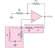
Oscillators
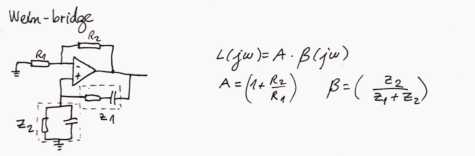
Closed Loop Gain
- is the closed loop gain of the system.
- is the open loop gain (with no feedback)
- is the feedback fraction, that feeds back a portion of the output voltage back to the input
Loop Gain
For oscillation, need unity gain, so angle therefore must be real, so also must be real.
Frequency Potential Divider ()
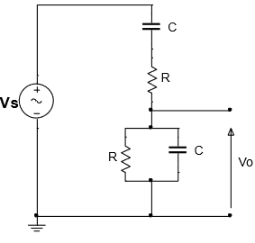
Frequency Potential Divider ()
Frequency of Unity Gain (0 phase shift)
60 Degrees of phase shift in CR network
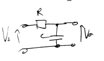
Transfer function of CR Network
= Gain of CR network
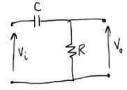
Transfer function of RC Network
= Gain of RC network
Transfer function of Inverse Frequency potential divider ()
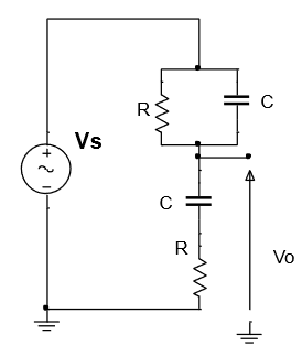
Transfer function of Inverse Frequency potential divider ()
Transfer function of Frequency potential divider (Inductor) ()
Transfer function of Frequency potential divider (Inductor) ()
Frequency of Unity Gain (0 phase shift) (Inductor)
BJT Transitors
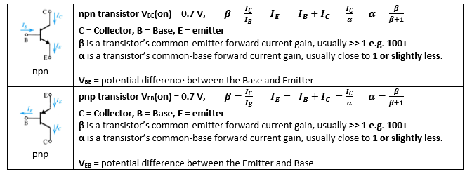
Common Emitter Forward Gain,
Common Base Forward current gain,
NPN Emitter Current
Emmitter Voltage Rule of Thumb
Thevin Resistance Rule of Thumb
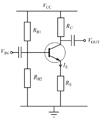
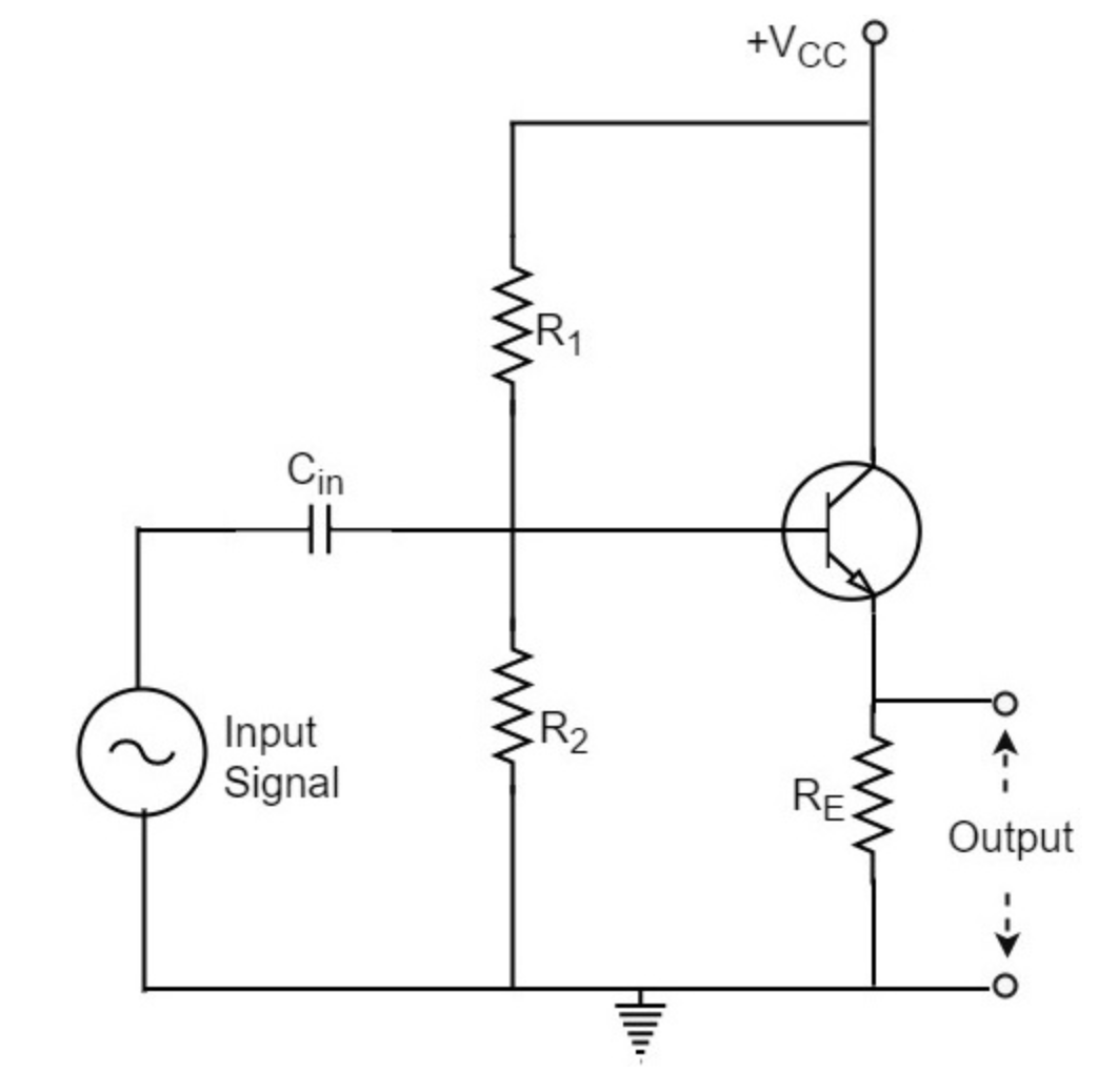
Four Resistor Bias Circuit
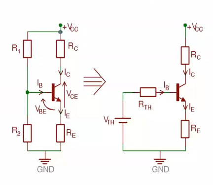
Four Resistor Bias Circuit
Transconductance
AC BJT Analysis
Amplifier Topologies
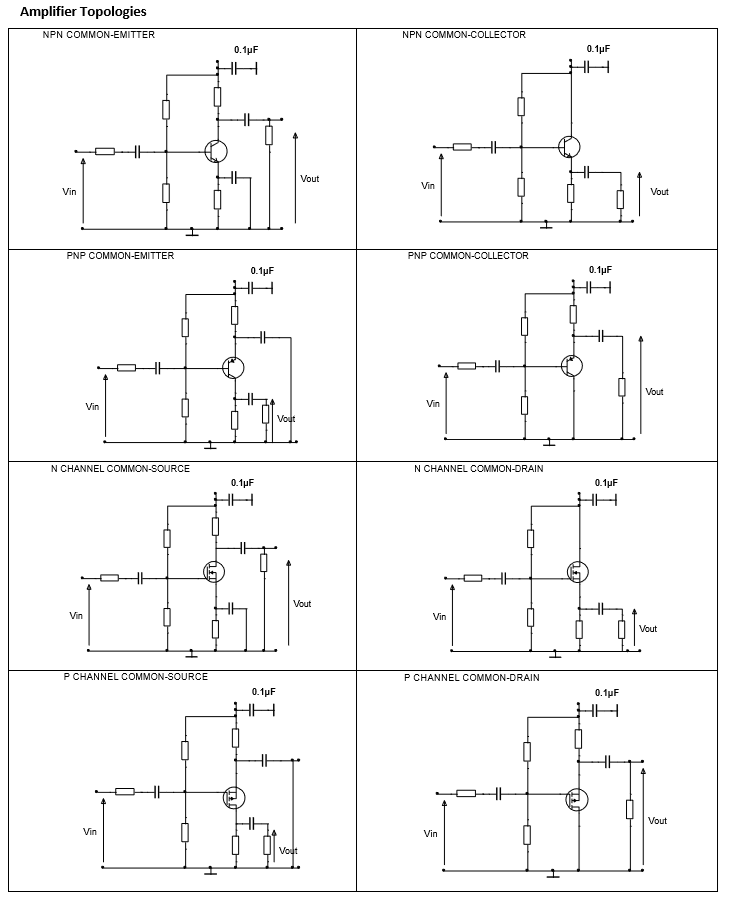
Transistor Input Impedance
Where = 25mV, = Collector current at Q point.
Gain of Collector Follower (Common Emitter) AC
Input Impedance of Collector Follower (Common Emitter)
Into the transistor
Output Impedance of Collector Follower (Common Emitter)
As current source has infinite impedance.
Emitter Follower (Common Collector)
- High Input, low ouput impedence
- High current gain
- So acts as impedence trasnformer and buffer
Voltage Gain of Emitter Follower (Common Collector)
as So low voltage gain, so instead current amplifier.
Current Gain of Emitter Follower (Common Collector)
Input Impedance of Emitter Follower (Common Collector)
Output Impedence of Emitter Follower (Common Collector)
Where = source input impedance
Output Impedence of Emitter Follower (Common Collector) Simple
Where = source input impedance
MOSFETs DC
No current through gate in MOSFET (as voltage controlled) (infinite input impedence)
Stages
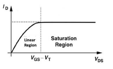
- Cut off (no current flows,
- Linear
- Saturation
Where = Threshold Voltage
Linear Region Drain Current
, where = transconductance constant
Saturation Drain Current
Saturation Drain Current -> VGS
Small Signal Model
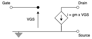
Transconductance
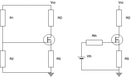
MOSFET Bias Network
Must check the two different values to see which ones are valid solutions.
MOSFET input impedence
As no current flows into gate
MOSFET Common Source
Similar to BJT common emmitter amplifier
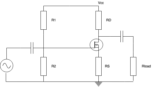
Overall Input Impedence
As two gate bias resistors act as impedances to input signals. Therefore used over BJTs when high impedence required.
Is actually in parallel with source (input) impedence if it has it.
Overall Output Impedance
What the load resistor sees.
As current source has infinite impedence, therefore is the only impedence seen.
Unless there is an which would be in parallel with .
Bypassed Gain
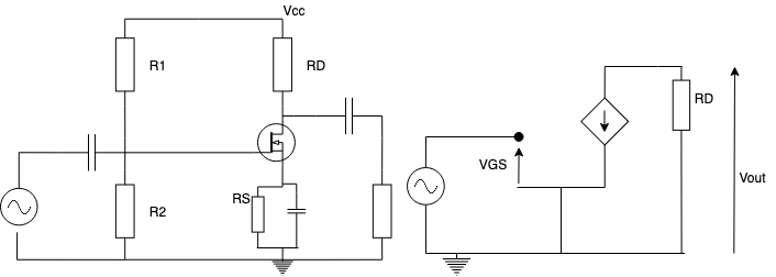
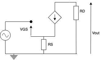
Common Drain (Source Follower)
Output Impedance
Differential Amplifier
Long tail pair:
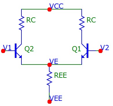
Modes Can operate in two modes.
- Differential (Amplfies Difference between two input signals)
- Common mode (Works similar to regular BJT amp)
Common Mode Same signal is connected to both input terminals.
- Ideal differential amp rejects common mode input, but not realistic
- Defined by CMRR
Better amps, have high ratio of differnetial to common gain, AKA Common Mode Rejection Ratio (CMRR).
Quiescent Current of Long Tail Pair
Current through shared emitter resistor, .
Biasing
and are grounded, therefore collector voltages are the same.
Collector Voltage of Grounded Long Tail Pair
And for matched transistors, .
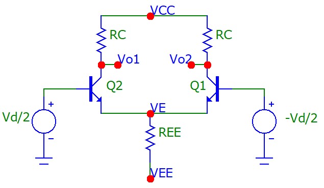
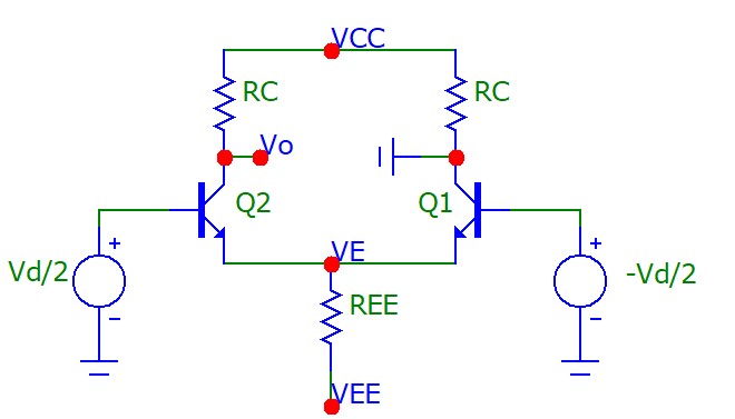
Differential Gain without ground
 Not really used
Differential Gain - Single Ended
Differential Input Resistance
Differential Output Resistance
Common Mode Gain
Common Mode Input Resistance
CMRR - Common Mode Rejection Ratio
Generalised Differential Amplifier Output
Both common mode and differential mode input signals are factored in.
Impedance Laplace
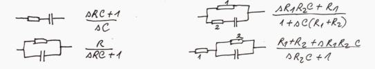
Resistor
Capacitor
Inductor
Resistor Capacitor Series
Resistor Capacitor Parallel
Resistor Inductor Series
Resistor Inductor Parallel
Op-Amps
Non-inverting Gain
Inverting Gain
Active Filter Gain
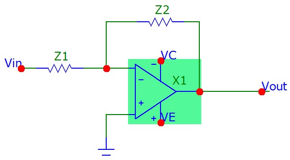
Active Filter Gain, Z2 = R2 || C
- Low Pass filter
- Cutoff where = Hz
Misc
Source Regulation
Fraction of change in load and input voltage
Load Regulation
Fraction of change in load to expected